BVLSI
Event-Aware Transient Level Shifter with a Detailed Study of the Cross-Coupled and Current-Mirror Level Shifters
Department of Electronics and Computer Science, Vidyalankar Institute of Technology, Mumbai, India
Published November 2026
Abstract
Level shifters are essential interface circuits in multi-voltage integrated systems because they translate logic signals between voltage domains while preserving signal integrity. This paper presents a comparative study framework for three CMOS level-shifter architectures: a conventional cross-coupled level shifter, a current-mirror level shifter, and an event-aware transient level shifter. The supplied circuit diagrams and transient plots are examined to describe their observed signal conversion behaviour. In the available current-mirror simulation plot, a low-voltage pulse with an approximate high level of 200 mV is associated with an output waveform reaching approximately 1.2 V. In the supplied event-aware transient plot, complementary input signals with a plotted high level near 500 mV drive complementary output waveforms with levels close to 1 V and 0 V. The plots indicate successful voltage-domain translation under the shown simulation conditions, while also showing finite transition times and waveform-edge effects. A quantitative ranking of the three architectures cannot yet be claimed because the cross-coupled baseline schematic/results and common simulation conditions have not been supplied. The paper therefore distinguishes observations supported by the supplied figures from measurements that must be completed before publication.
Keywords: Level shifter; CMOS; cross-coupled level shifter; current mirror; event-aware transient level shifter; transient analysis; low-voltage circuit
1Introduction
Modern integrated circuits frequently combine blocks that operate at different supply voltages to reduce power consumption or accommodate different device requirements. Signals exchanged between these blocks may not meet the receiving circuit's logic-level requirements. A level shifter translates a signal from one voltage domain to another and is therefore an important building block in low-power digital systems, memory interfaces, sensor interfaces, and mixed-voltage integrated circuits. Multi-voltage design has become a standard technique for reducing power in integrated circuits, because dynamic power scales with the square of the supply voltage while performance-critical blocks may still require a higher supply [1, 2]. In such systems a low-voltage block can drive a higher-voltage block only if the interface restores the signal to a level that the receiving gates interpret correctly. A low-voltage input that cannot fully turn off the PMOS devices of a high-voltage gate causes large static short-circuit current, so a level shifter is needed at every low-to-high domain crossing [1].
A level shifter must be assessed using more than its ability to produce a high output. Relevant metrics include input and output voltage ranges, propagation delay, rise and fall times, static and dynamic power, energy per transition, output swing, area, robustness across process-voltage-temperature (PVT) variations, and correct operation for both input transitions. Different circuit topologies trade off these characteristics. This project compares a cross-coupled architecture, a current-mirror architecture, and an event-aware transient architecture using circuit-level simulation.
The difficulty of level shifting increases as the input supply approaches the device threshold voltage. A simple cross-coupled level shifter may then fail to switch because the input-driven pull-down devices cannot overpower the cross-coupled pull-up devices. This limitation has motivated current-mirror based and logic-error-correcting level shifters, as well as designs aimed at high speed and wide-range conversion [3]–[6]. Wide-range conversion, low delay, low static current, and small area are competing objectives, and no single topology is optimal for every supply pair.
The aim of this paper is to document the three-topology comparison and analyse the transient waveforms currently available. Since the supplied evidence includes current-mirror and event-aware circuit/result images but does not include a complete cross-coupled baseline result set or numerical measurements for all topologies, this draft does not claim a definitive winner. A fair comparison requires all architectures to be simulated with matched supply voltages, input frequency, load capacitance, device models, temperature, and measurement definitions.
The main contributions of this work are: (i) a qualitative operating-principle study of the cross-coupled, current-mirror, and event-aware transient level shifters, including a first-order sizing relation for the cross-coupled stage; (ii) a set of measurement definitions and a fair-comparison procedure that can be applied identically to all three topologies; and (iii) an analysis of the transient waveforms supplied for the current-mirror and event-aware circuits, with the limits of what can be concluded from them stated explicitly.
The remainder of the paper is organised as follows. Section 2 reviews related work and the comparison criteria, Section 3 describes the methodology and the supplied simulation evidence, Section 4 presents and discusses the results, and Section 5 concludes the paper.
2Literature survey and comparison criteria
Prior CMOS VLSI and digital integrated-circuit texts describe the role of transistor sizing, regenerative feedback, parasitic capacitance, and switching current in determining circuit performance [7, 8]. These principles provide the background for evaluating level shifters. The comparison in this paper therefore identifies, for each topology, the operating principle, the expected behaviour with respect to supply voltage, and the data that must be measured for a fair comparison, namely delay, power, load, process technology, and limitations.
Level-shifter research has followed several directions. Lütkemeier and Rückert [3] proposed a level shifter based on a Wilson current mirror to convert signals from subthreshold to above-threshold voltage levels, addressing the difficulty that simple cross-coupled stages have when the input swing is low. Osaki et al. [4] introduced a low-power level shifter with logic-error correction for extremely low-voltage digital CMOS circuits, in which the added mechanism corrects logic errors that arise at very small input voltages. Hosseini et al. [5] reported a high-speed and power-efficient level shifter for dual-supply applications, and Lanuzza et al. [6] addressed fast and wide-range voltage conversion in multi-supply voltage designs. These works share a common message: a level shifter must be judged by its conversion range, delay, power, and static current together, and the results depend strongly on the supply pair, load, and process technology.
Studies of logic styles in general, such as that of Zimmermann and Fichtner [9], similarly show that the preferred style depends on supply voltage, load, and design goal. Direct numerical comparison across papers is therefore unreliable unless the circuits are simulated again under the same conditions, as recommended in standard CMOS design texts [7, 10]. This is the approach adopted here.
2.1Cross-coupled level shifter
A conventional cross-coupled level shifter commonly uses a pair of cross-coupled pull-up devices to reinforce one of two internal nodes. Input-controlled pull-down devices steer the internal nodes, and regenerative feedback helps establish the translated logic state. Its strengths can include a strong output state and static regeneration. Potential limitations include contention during switching, delay dependent on device sizing and input slew, and reduced robustness when the input-domain signal is too weak to control the pull-down devices reliably.
The operation can be understood by considering a low-to-high input transition. When the input rises to the low-voltage supply VDDL, the input-driven NMOS device pulls one internal node down. That node must fall far enough for the opposite cross-coupled PMOS device, supplied from the high-voltage rail VDDH, to turn on and latch the new state. Because the PMOS device that initially holds the node high is still conducting, the NMOS and PMOS devices contend until the node falls below the switching threshold of the feedback pair. A first-order square-law estimate, with the PMOS device fully on and the NMOS gate at VDDL, gives the condition for a successful transition:
Here (W/L)N and (W/L)P are the width-to-length ratios of the pull-down and pull-up devices, μn and μp are the carrier mobilities, and Vtn and Vtp are the threshold voltages. The relation shows why the design becomes difficult as VDDL approaches Vtn: the denominator tends to zero and the required width ratio grows without bound, so the pull-down devices must be made much wider than the pull-up devices. This increases area and input capacitance and slows the opposite transition. It also explains the usual trade-off between contention current, switching delay, and robustness to process variation discussed in [7, 10]. Equation (1) is a first-order guide only and must be verified by simulation with the actual device models.
2.2Current-mirror level shifter
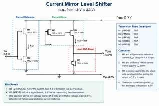
A current-mirror-based architecture uses current relationships and transistor biasing to control internal nodes and generate a translated output. Its behaviour depends on transistor dimensions, current levels, device operating regions, parasitic capacitances, and the loading at the output. The current-mirror level shifter is shown in Figure 1. The supplied schematic is labelled as a current-mirror level shifter, and its transient plot provides the available evidence for this topology. The topology should be assessed for voltage translation, edge timing, static current, and power under matched test conditions.
In a current-mirror level shifter, the low-voltage input modulates a branch current instead of directly opposing a latch. The mirror copies this current into the high-voltage branch, where it develops a voltage across a load device that is then restored by an output inverter or buffer. Because the conversion relies on a mirrored current, the circuit can operate with smaller input swings than a simple cross-coupled stage, at the cost of a bias current that may flow in at least one logic state and therefore raises static power [3]. The mirror ratio, transistor sizing, and output loading set both the speed and the output swing.
2.3Event-aware transient level shifter
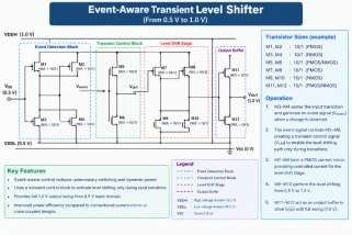
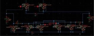
An event-aware transient architecture uses transient or event-triggered paths to assist switching between logic states. Such approaches may accelerate transitions by providing a temporary switching response, but the actual benefit depends on circuit implementation and timing. The supplied schematic includes complementary input/output-labelled nodes and transient-circuit elements. Its waveform should be checked for correct complementary operation, pulse integrity, overshoot/undershoot, and steady-state restoration.
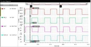
The event-aware transient level shifter is shown in Figure 2. The architecture studied here uses complementary inputs, IN and IN_B, and complementary outputs, OUT and OUT_B, as seen in the supplied schematic and waveform. Using both polarities allows each output node to be driven toward the appropriate rail at a transition. A typical benefit sought from event-triggered assistance is that the extra drive is active only around the input edges, so the static contention current is expected to be lower than in an always-ratioed latch, although this must be confirmed by supply-current measurements. The price is additional circuit elements and the need to generate or distribute complementary input signals in the low-voltage domain.
2.4Metrics for a fair comparison
Table 1 lists the metrics adopted for the comparison, how each is measured, and why it matters. Their definitions are fixed in advance so that all three topologies are judged identically.
| Metric | How to measure | Why it matters |
|---|---|---|
| Voltage translation | Record input and output low/high levels | Confirms compatibility between voltage domains |
| Propagation delay | Measure input 50% crossing to output 50% crossing | Measures response speed |
| Rise/fall time | Measure output 10–90% and 90–10% intervals | Shows edge quality and switching strength |
| Power/energy | Integrate supply current over steady and switching intervals | Compares efficiency |
| Output integrity | Check overshoot, undershoot, ripple and logic levels | Detects transient errors |
| Robustness | Repeat over PVT corners and load values | Tests practical reliability |
The propagation delay is taken as the average of the low-to-high and high-to-low delays measured between the 50% points of the input and output waveforms:
The average power is obtained from the supply current drawn from each supply rail over an integer number of input periods, and the power-delay product and the energy per cycle follow from it:
Here fin is the input frequency. Output integrity is quantified by the output high level, the output low level, and the overshoot and undershoot beyond the rails, while the static current is measured during an interval in which the inputs are held constant. A level shifter that meets these definitions across PVT corners and load capacitances can be regarded as robust.
3Proposed methodology and discussion
The comparison is organised around circuit implementation and transient simulation. Each topology should be implemented using the same technology/model library and the same nominal supply domains. Apply the same periodic input stimulus, set identical output load capacitance, and simulate long enough to observe several complete cycles after start-up. Save the transistor-level schematic, transient waveforms, and supply-current traces for each design. For every topology, record the input low/high levels, output low/high levels, propagation delay for rising and falling transitions, rise/fall times, average supply power, and energy per cycle. Use the same threshold convention for every circuit. If the event-aware design uses complementary inputs, document how these are generated and ensure the baseline circuits are driven using equivalent logical information. Run additional tests at different frequencies, output loads, supply voltages, and PVT corners before drawing broad conclusions.
3.1Simulation evidence supplied for this draft
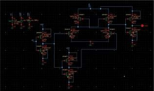
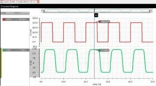
The supplied images show a current-mirror level-shifter schematic and its transient response (Figures 3 and 4), as well as an event-aware transient level-shifter schematic and its transient response (Figures 5 and 6). The current-mirror plot has a 0–50 ns time axis and shows an input-like trace with a high level around 200 mV and an output trace reaching approximately 1.2 V. The event-aware plot also spans approximately 0–50 ns; the displayed input and complementary input switch around 0 and 500 mV, while the output and complementary output traces switch between levels close to 0 and 1 V. These values are visual estimates read from the plotted scales, not extracted simulator measurements.
3.2Simulation setup and measurement procedure
For each topology the schematic is entered in a circuit simulator, and a transient analysis is run with the same device model library and process technology. The input source is a periodic pulse whose high level equals the low-voltage supply of the circuit under test and whose period is the same for every design. In the supplied plots the input period is approximately 10 ns, so the 0–50 ns window contains about five complete cycles. The output node is loaded with an identical capacitor, and the supply current of each rail is recorded together with the waveforms. Delay is evaluated at the 50% crossing points, and rise and fall times between the 10% and 90% levels of the output swing, using the definitions of Section 2.4. Measurements are taken from cycles after start-up to avoid initial-condition artefacts and are averaged over several cycles. Once the baseline conditions are fixed, the supply voltage, input frequency, load capacitance, temperature, and process corner are swept one at a time to examine robustness.
4Experimental results and discussion
4.1Current-mirror level shifter
In Figure 4, the input waveform reaches an indicated high level of about 200 mV, while the output waveform reaches approximately 1.199 V at the displayed cursor. This supports the observation that the simulated circuit produces a higher-voltage output domain than the low-voltage input domain under the shown setup. The output edges are not instantaneous; rounded transitions are visible, consistent with finite transistor drive and parasitic/load capacitance. The figure alone does not provide reliable numerical delay, rise/fall time, power, or output-load information. These values should be measured directly from the simulator before final submission.
4.2Event-aware transient level shifter
In Figure 6, IN and IN_B appear as complementary pulse signals with a plotted high level near 500 mV. OUT and OUT_B appear complementary, with one output high near 1 V while the other is low near 0 V, followed by a state reversal. This indicates complementary voltage- domain translation in the displayed transient simulation. Small edge disturbances are visible around transitions; their magnitude and duration should be quantified from simulator data rather than inferred from the screenshot. The supplied figure does not by itself establish a speed or power advantage over the other topologies.
4.3Cross-topology comparison status
The current evidence is sufficient for a qualitative description of the current-mirror and event-aware transient waveforms, but it is not sufficient for a complete numerical comparison of all three architectures. No cross-coupled schematic or transient result was included in the supplied images. In addition, the plotted circuits do not visibly establish that the supply conditions, device models, output loads, input frequency, and measurement thresholds are identical. Consequently, no claims such as 'fastest', 'lowest power', or 'best overall' should be made until a matched simulation campaign has been completed.
Table 2 summarises, for each topology, the evidence currently available, the observation that evidence supports, and the data that are still required.
| Topology | Evidence currently available | Supported observation | Data still required |
|---|---|---|---|
| Cross-coupled | No schematic/waveform supplied | No result claim can be made | Schematic, transient plot, delay, power, output levels |
| Current-mirror | Schematic and transient plot | Input high ≈0.2 V; output cursor ≈1.199 V in shown plot | Exact delay, rise/fall time, power, load, supply settings |
| Event-aware transient | Schematic and transient plot | Complementary inputs around 0/0.5 V; outputs around 0/1 V | Exact delay, edge disturbance, power, load, supply settings |
4.4Quantities derived from the supplied plots
Although the supplied plots do not permit exact delay or power extraction, several useful quantities follow directly from the plotted voltage levels and the cursor labels. They are summarised in Table 3 and should be regarded as visual estimates, not simulator measurements.
| Quantity | Current-mirror | Event-aware transient |
|---|---|---|
| Input high level | ≈0.2 V | ≈0.5 V |
| Output high level | ≈1.2 V | ≈1.0 V |
| Output low level | ≈0 V | ≈0 V |
| Input period | ≈10 ns | ≈10 ns |
| Cycles in 0–50 ns | ≈5 | ≈5 |
| Step-up ratio | ≈6 | ≈2 |
| Output form | Single-ended | Complementary |
The current-mirror circuit steps a 0.2 V input up to about 1.2 V, a ratio of about six, whereas the event-aware circuit steps 0.5 V to about 1 V, a ratio of about two. In both plots the output low level is close to 0 V; the event-aware plot reads only a few microvolts on OUT_B at the cursor, which indicates that the low level sits essentially at the rail. Because the input amplitude, output supply, and conversion ratio differ between the two plots, they must not be used to rank the circuits. They show only that each circuit performs its own conversion under its own conditions.
4.5Qualitative comparison of the topologies
Table 4 summarises the expected qualitative behaviour of the three topologies on the basis of the operating principles discussed in Section 2. These entries are design expectations drawn from circuit theory [3, 7, 10], not simulated results, and each must be confirmed by the matched simulation campaign.
| Topology | Mechanism | Expected strength | Main concern |
|---|---|---|---|
| Cross-coupled | Regenerative PMOS pair with NMOS pull-down | Strong output state; no bias current expected | Contention when VDDL is near Vtn |
| Current-mirror | Input current mirrored into high-voltage branch | Operation with smaller input swing | Possible bias current and area |
| Event-aware transient | Complementary inputs with transient assist | Complementary outputs; assisted edges | Extra elements; complementary inputs needed |
4.6Limitations
The main limitation of the present study is the absence of simulated data for the cross-coupled level shifter and of exact numerical measurements for all three circuits. In addition, the plotted conditions differ between the two available circuits, and the figures do not state the load, device sizes, or process corner. The paper therefore provides a comparison framework and qualitative evidence rather than a ranking. Extending the work with matched simulations will turn the expectations of Table 4 into measured results.
5Conclusion and future work
This draft documents a comparative investigation of cross-coupled, current-mirror, and event-aware transient level shifters. The supplied current-mirror waveform shows a low-voltage input pulse and an output reaching approximately 1.2 V. The supplied event-aware waveform shows complementary output switching near 0 V and 1 V in response to complementary inputs near 0 V and 0.5 V. These observations indicate voltage translation in the shown simulations, but screenshots alone are insufficient to quantify delay, power, energy, or robustness. The study also contributes a first-order sizing relation for the cross-coupled stage (Equation 1), a consistent set of metric definitions (Equations 2–5), and a qualitative comparison (Table 4) that can serve as a template for the matched simulations.
The principal next step is to complete the cross-coupled baseline simulation and repeat all three designs under matched conditions. Numerical measurements should be extracted from simulator waveforms, tabulated using consistent definitions, and validated across multiple cycles. Additional testing should include output-load variation, input-frequency variation, supply-voltage variation, and process-voltage-temperature corners. Only after these measurements are available can the paper support a defensible ranking of the three architectures.
References
- [1]Kursun V, Friedman EG. Multi-voltage CMOS circuit design. Chichester: Wiley; 2006.
- [2]Chandrakasan AP, Sheng S, Brodersen RW. Low-power CMOS digital design. IEEE Journal of Solid-State Circuits. 1992;27(4):473–484.
- [3]Lütkemeier S, Rückert U. A subthreshold to above-threshold level shifter comprising a Wilson current mirror. IEEE Transactions on Circuits and Systems II: Express Briefs. 2010;57(9):721–724.
- [4]Osaki Y, Hirose T, Kuroki N, Numa M. A low-power level shifter with logic error correction for extremely low-voltage digital CMOS LSIs. IEEE Journal of Solid-State Circuits. 2012;47(7):1776–1783.
- [5]Hosseini SR, Saberi M, Lotfi R. A high-speed and power-efficient voltage level shifter for dual-supply applications. IEEE Transactions on Very Large Scale Integration (VLSI) Systems. 2017;25(3):1154–1158.
- [6]Lanuzza M, Corsonello P, Perri S. Fast and wide range voltage conversion in multisupply voltage designs. IEEE Transactions on Very Large Scale Integration (VLSI) Systems. 2015;23(2):388–391.
- [7]Rabaey JM, Chandrakasan A, Nikolić B. Digital integrated circuits: A design perspective. 2nd ed. Upper Saddle River (NJ): Prentice Hall; 2003.
- [8]Weste NHE, Harris DM. CMOS VLSI design: A circuits and systems perspective. 4th ed. Boston (MA): Addison-Wesley; 2011.
- [9]Zimmermann R, Fichtner W. Low-power logic styles: CMOS versus pass-transistor logic. IEEE Journal of Solid-State Circuits. 1997;32(7):1079–1090.
- [10]Kang SM, Leblebici Y. CMOS digital integrated circuits: Analysis and design. 4th ed. New York: McGraw-Hill; 2014.